
RTLCoding & FPGA Design
Indeemicro Technologies institute is among the top 10 Indeemicro training institutes in India. At Indeemicro, we understand the changing demands in the field of Indeemicro.
RTL Coding and FPGA Design Training / FPGA Training Courses
RTL Coding and FPGA Design course has been designed to help to the beginners in the area of RTL coding and FPGA design. The course gives you the foundation for FPGA design in Embedded Systems along with practical design skills. By end of the course you will learn what FPGA, how to select the best FPGA architecture for a given application, solve critical digital design problems using FPGAs. As a part of the course, you will also learn to use FPGA development tools to complete several example designs, including a custom processor.
If you are thinking of a career in Electronics Design or as an engineer looking at a career change, this is a great course to enhance your career opportunities.
Eligibility
- B.E/B.Tech in ECE/EEE.
- M.E/M.Tech/M.S in VLSI/Embedded Systems/Digital Electronics.
Course Duration
- 5 Months
Course Highlights
- Deep understanding of digital logic design.
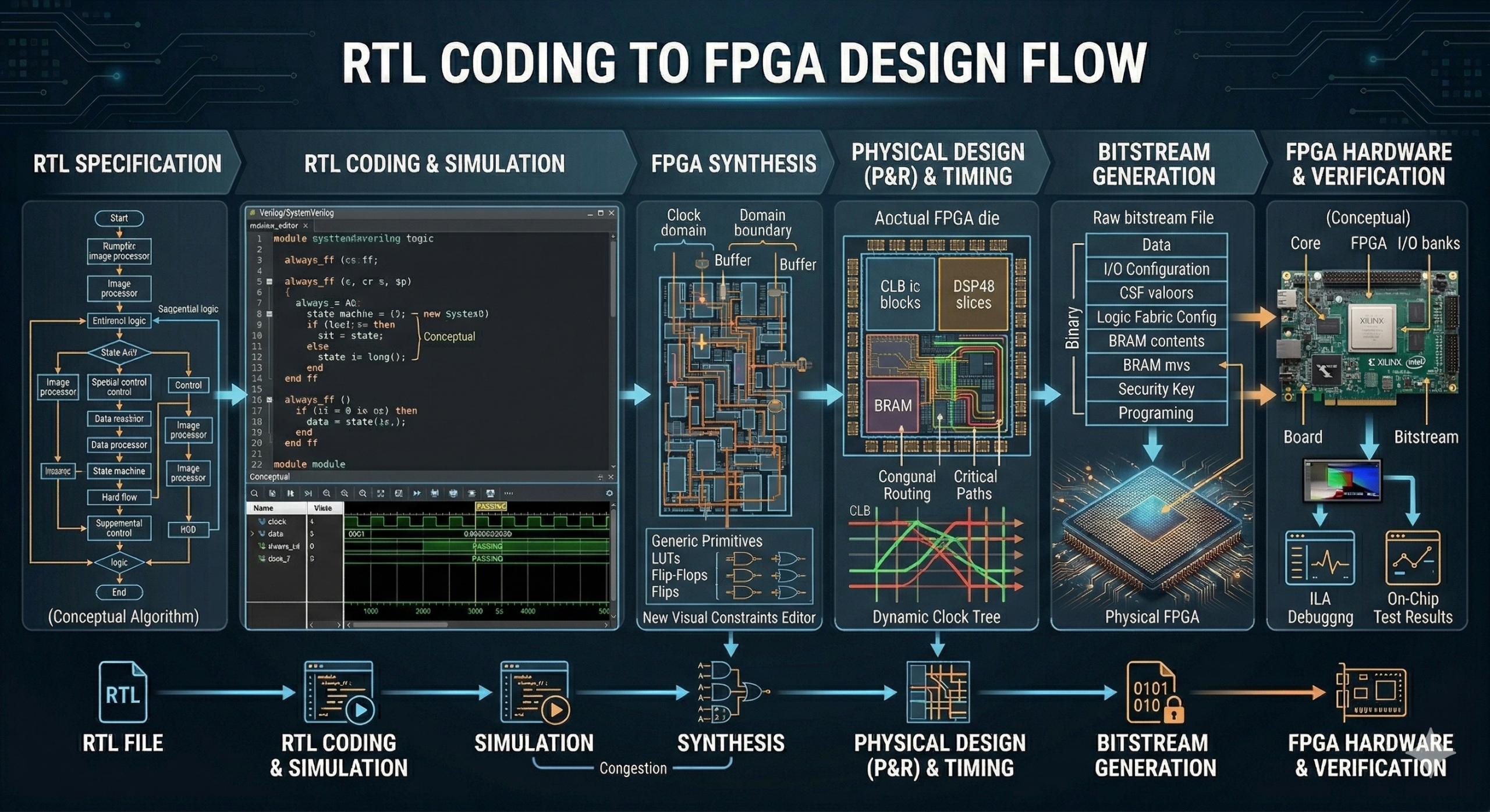
- Knowledge of FPGA/ASIC design flow.
- In depth knowledge of Verilog HDL – RTL coding & synthesis.
- Fare understanding of creating power friendly RTL design.
- Good understanding of FPGA implementation and debugging on Xilinx evaluation board.
- Acquire skills to do minor/major projects.
- 24×7 Lab Support with Lab practice handouts and course material delivery.
- Industry standard project execution, Lab practice and theory sessions under the guidance of industry expert with 12+ years of experience.
- Soft skills development, complete suite of job oriented ASIC Verification training with 100% placement assistance.
FPGA Design, RTL Coding & RTL Design Training Institute
Course Curriculum
- Introduction to Unix/Linux OS Architecture
- UNIX Directory Structures and Unix Commands
- UNIX Shells
- LAB Exercises
- Importance and advantages of digital electronics
- Digital Number System, Binary logic gates & Boolean algebra
- Combinational and Sequential circuit designs
- Finite state machine optimization
- What is FPGA? What is ASIC?
- Overview of FPGA/ASIC/SOC design flow
- FPGA Vs ASIC comparison summary
- How to choose between FPGA or ASIC
- Introduction to RTL coding
- Overview of digital design with verilog HDL
- Design modelling with examples
- Tasks and functions
- RTL Simulation and synthesis
- Creating power friendly RTL & Timing analysis
- Module level test bench development
- RTL design optimization techniques
- Read only Memories (ROM)
- PALs & PALs
- CPLDs & FPGAs
- FPGA Architecture
- Dual port memory – Example design
- FPGA design Flow
- Bit file generation & downloading the Hex file to FPGA device
- FPGA validation through chipscope & DS5 debugger
- Project work and board bring up
- Overview of 7 series FPGA architecture
- Introduction to Zynq FPGA-SoC — SoCs with Hardware and Software programmability
- Efficient FPGA RTL coding for design synthesis & Implementation
- Xilinx tool introduction & Installation
- RTL simulation – Qsim from Mentor graphics
- Hands-on experience in using vivado design suite for design synthesis and Implementation
- Hands-on experience in using chipscope and DS5 debugger for debugging functioality failures